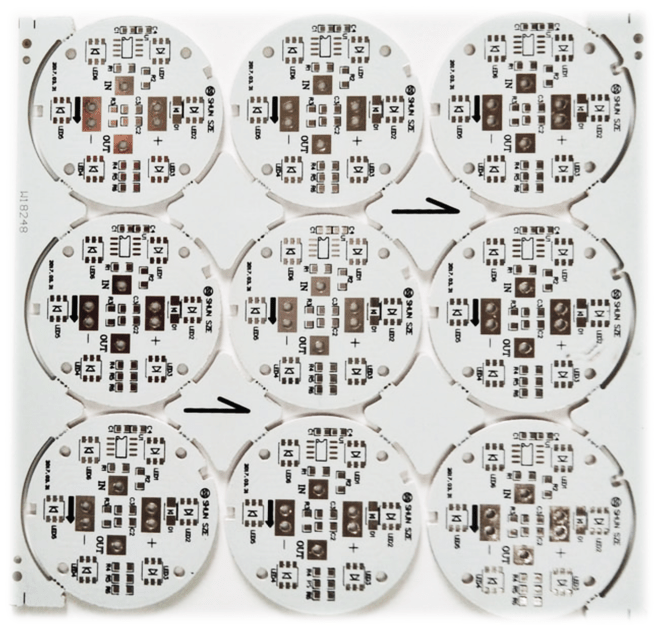
Aluminum PCB
Alunimum PCB
- 1-2 layer Aluminum PCB
- Board Thickness:0.8 – 4MM
- Copper Thickness: 1-4OZ
- 2-3 Days Fast Aluminum PCB Prototype
- 7-10 Days Fast Production Lead Time for upto 100+m2/order


Content Table
3.1 Aluminum Production Procedure Flow-chart
3.1.1 Aluminum PCB Raw Material Cutting
3.1.3 Dry/Wet film imaging of circuit layer
3.1.4 Aluminum PCB Raw Material Cutting
3.1.5 Acid/alkaline etching of circuit layer
3.1.6 Screen printing solder mask, character
3.1.7 V-CUT,Profiling of Aluminum PCB
3.1.8 Aluminum PCB Testing & OSP
3.1.9 Aluminum PCB FQC, FQA, Packaging, Shipping
3.2 Technics process requirements of aluminum PCB
3.2 Precautions for Aluminum PCB Production
4.1 Objects, scope of application, definition
4.2 Technical Parameters of Aluminum PCB
4.3 Aluminum PCB Material Requirements
4.4 Thermal Design Requirements of Aluminum PCB
4.5 Selection Requirements of Component Library
4.6 Layout Requirements of Aluminum PCB components
4.7 Trace Layout Rules of Aluminum PCB
4.8 Design Requirements of Fixed Hole, Mounting Hole
& Through Hole of Aluminum PCB
4.9 Design Requirements of Fiducial Marks
4.10 Silkscreen Design Requirements
4.11 Dimension & Shape Requirements of Aluminum PCB
What is Aluminum PCB
Introduction of Aluminum PCB
Aluminum PCB is the PCB type that used the low alloyed Al-Mg-Si with high plasticity alloy plate as the substrate material that has better thermal conductivity, electrical insulation, and machining performance, compared with the traditional FR4 PCB.
Similar to other types of PCBs, Aluminum PCB is structured by the conductive layer (copper layer); insulation layer (dielectric layer); and the substrate layer.
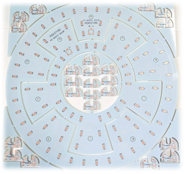
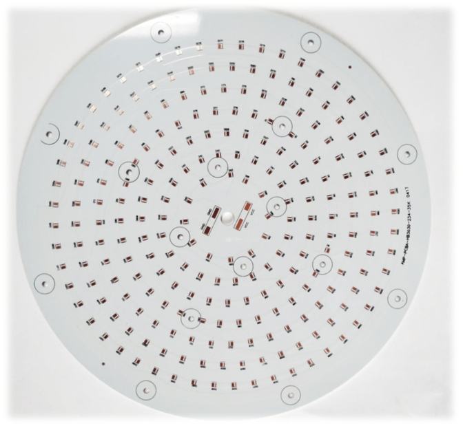
Aluminum PCB is capable to stand higher current with the same thickness and line width. Aluminum PCB is able to withstand voltage up to 4500V and thermal conductivity is more than 2.0. At present, aluminum PCB is the most common type for LED lighting PCB applications.
Common LED PCB has two sides. The top side with white solder mask is used for soldering SMD LED beads, and the other side normally has no solder mask and showing as aluminum metal color. If there is a demand for high-power heat dissipation, the aluminum base can also be coated with a thermal conductive silicone grease layer to connect with the installed heatsinks for better heat dissipation.
Pros & Cons of Aluminum PCB
Pros of Aluminum PCB
- Meet ROHS requirements;
- It is more suitable for SMT process;
- In the circuit design scheme, the thermal diffusion is treated effectively to reduce the operating temperature of the module, prolong the service life, and improve the power density and reliability;
- Reduce the assembly of radiator and other hardware (including thermal interface materials), reduce product volume, and reduce hardware and assembly costs;
- The power circuit and control circuit are optimized;
- Replace the fragile ceramic substrates for better mechanical durability
Cons of Aluminum PCB
- The cost is high. (At FastPCBunion.com, we could help you reduce the cost, and make sure that switch from FR4 to Aluminum PCB would not cost you any extra for your LED appliances.)
- At present, the design of Aluminum PCB is mainly limited to 1-2 layer board, due to the mainstream manufacturing capability.
- It is easy to have problems in electrical strength and withstand voltage. (At FastPCBunion.com, we have resolved the problem)
Suitable Appliances of Aluminum PCB
LED lighting products
Currently, aluminum PCB has been widely using for lighting PCB, especially LED PCB. Besides lighting appliance, there are main other senarios that are suitable for Aluminum PCB.
Audio equipment
Input, output amplifier, balanced amplifier, audio amplifier, pre-amplifier, power amplifier, etc.
Power supply equipment
Switch regulator ` DC / AC converter ` SW regulator, etc.
Communication electronic equipment
High frequency amplifier ‘filter electrical’ transmitting circuit.
Office automation equipment
Motor driver, etc.
Automobile
Electronic regulator, igniter, power controller, etc.
Computer
CPU board, floppy disk driver, power supply device, etc.
Power module
Converter, solid-state relay, rectifier bridge, etc.
Aluminum PCB Classification
1、 Traditional aluminum PCB
Traditional aluminum PCB is a hard PCB made of aluminum plate, insulating layer, and the conductive layer.
According to the manufacturing process, aluminum PCB can be divided into: tin spraying aluminum PCB, oxidation-resistant aluminum PCB, silver plating aluminum PCB, immersion gold aluminum PCB, etc.

According to the appliances, aluminum PCB can be divided into: street lamp aluminum PCB, fluorescent lamp aluminum PCB, LB aluminum PCB, COB aluminum PCB, packaged aluminum PCB, bulb lamp aluminum PCB, power supply aluminum PCB, automobile aluminum PCB, etc.
2、 Flexible aluminum PCB
One of the latest developments of IMS materials is flexible dielectrics. These materials provide excellent electrical insulation, flexibility, and thermal conductivity. When applied to flexible aluminum materials such as 5754 or similar, products can be formed to achieve various shapes and angles, which can eliminate expensive fixtures, cables, and connectors. Although these materials are flexible, they are designed to bend into place and remain in place.
3、 Mixed aluminum PCB
In the “hybrid” IMS structure, the “sub-assemblies” of nonthermal materials are treated independently, and then Amitron hybrid IMS PCBs are bonded to the aluminum substrate with thermal materials. The most common structure is a 2-layer or 4-layer sub-assembly made of traditional FR4. Bonding this layer to an aluminum substrate with a thermoelectric medium can help heat dissipation, improve rigidity, and act as a shield. Other benefits include:
a. It’s cheaper than building all the heat-conducting materials.
b. Provides better thermal performance than standard FR-4 products.
c. Expensive radiators and associated assembly steps can be eliminated.
d. It can be used in RF applications requiring RF loss characteristics of PTFE surface layer.
e. The use of component windows in aluminum to accommodate through-hole assemblies allows connectors and cables to pass connectors through the substrate while welding fillets to create a seal without the need for special gaskets or other expensive adapters.
4、 Multilayer aluminum PCB
In the high-performance power market, multi-layer IMS PCB is made of multilayer thermal conductive dielectrics. These structures have one or more layers of circuits embedded in dielectrics, and blind holes are used as thermal through holes or signal paths. Although it is more expensive and less efficient to transfer heat in a single layer design, they provide a simple and effective cooling solution for more complex designs.
5、 Through-hole aluminum PCB
In the most complex structures, a layer of aluminum can form the “core” of a multilayer thermal structure. Prior to lamination, aluminum is electroplated and dielectric-filled. Thermal materials or subassemblies can be laminated to both sides of the aluminum using a thermal bonding material. Once laminated, the finished component is similar to the traditional multilayer aluminum substrate through drilling. Electroplated vias pass through gaps in aluminum to maintain electrical insulation. Alternatively, copper cores may allow direct electrical connections and insulated through holes.
Fast PCB Union - The Aluminum PCB Manufacturer
Fast PCB Union Co. LTD has been specialized in Aluminum PCB manufacturing field for over 10 year.
Our Aluminum PCB products including High power aluminum PCB to suit your high power high dissipation requirements for your design, and the normal consumer-grade aluminum PCBs to satisfy your requirement on aluminum PCB cost without sacrifice the quality.
Focusing on the R&D and manufacturing of aluminum pcb for 10+ years, Fast PCB union achieved the first breakthrough in mass production of bendable aluminum pcb in China, ultra long 1.5 m aluminum pcb, ultra thin 0.2 mm aluminum pcb, ultra high thermal conductivity (122W) ALC aluminum pcb, copper core PCB with thermoelectric separation technology, etc.
Our Technical Capability
Technical Object | Capability & specification |
Material | Aluminum substrate 1-2 Layer |
Thermal conductivity | 1.0W/1.5W/2.0W/122W |
Thickness | 0.3~5.0MM |
Surface Finishing | Lead-free HASL / Immersion Gold /OSP |
Max. Panel size | 1500*500MM |
Min. Panel size | 5*5MM |
Min line width | 0.25MM (10mil) |
Min line gap | 0.25MM (10mil) |
Minimum aperture | ∮1.6mm |
E-T Test | 100% Automated short circuit test |
Technical Object | Capability & specification |
Plate warp rate | <=0.5% (350*350mm) |
Withstand voltage | AC1500-4000V |
Copper Foil Thickness | 18um / 35um / 70um / 105um |
Molding method | CNC /Die punching/ V-CUT |
External tolerance | CNC: ±0.1~0.15MM Die punching:±0.125MM |
Type of resistance welding | White or customized |
Production process | Exposure process |
Monthly capacity | 20000 square meters |
Lead Time | Sample: 2-4 days / batch: 1~3 weeks. |
The Preferred Aluminum PCB Supplier in China
Fast PCB Union has been proudly servicing Aluminum PCB needs in China and Globally among the cutting-edge materials. Accordingly to your appliances & budget, we will provide you the best option from the market available Aluminum PCB substrate materials to produce your Aluminum PCB in the most cost-effective manner.
Founded in July 2004, Fast PCB Union, has a complete Alunimum PCB & MCPCB manufacturing factory with a total investment of 4.5 million US dollars and more than 200 employees. In 2017, it was awarded the qualification of China’s national high-tech enterprise. At present, our aluminum PCB products are widely used in LED lighting, high-power power supply, automobile lamp lighting, new energy battery, automobile charging pile, etc.
The company pursues the business philosophy of “integrity based, innovation and further development”, attaches great importance to R&D micro innovation, and has China’s national practical patent certificate. “Quality as the root, create value for customers” is the company’s service tenet. At present, we have obtained ISO 9001:2015 quality system certification, SGS certification and UL certification. The company has passed IATF16949 automobile industry technical specification certification.
Along the way, we have been recognized by many well-known brand customers. Thanks for having you all the way, we will work harder!
Aluminum PCB Substrate Materials
Selection of Raw Materials for Aluminum PCB
There are mainly 1000 series, 5000 Series and 6000 series aluminum based plates in common use. The basic characteristics of these three series aluminum materials are as follows:

① 1000 series (typical models – 1050, 1060, 1070)
1000 series aluminum plate is also known as pure aluminum plate. In all series, 1000 series aluminum content is the most, and the purity can reach more than 99.00%. Because it does not contain other technical elements, the production process is relatively simple and the price is relatively cheap. It is the most commonly used series in conventional industries. Most of the 1050 and 1060 series are in circulation on the market. 1000 series aluminum plate is based on the last two digits to determine the minimum aluminum content of this series. For example, the last two digits of 1050 series are 50. According to the international brand naming principle, its aluminum content must reach 99.5%, and the top is the qualified product. In China’s aluminum alloy technical standard (GB / t3880-2006), the aluminum content of 1050 is 99.5%. In the same way, the aluminum content of 1060 series aluminum plate must reach more than 99.6%.
② 5000 Series (typical models – 5052, 5005, 5083, 5A05 Series)
5000 series aluminum plate belongs to the common alloy aluminum plate series, the main element is magnesium, the magnesium content is between 3-5%, which is also known as aluminum magnesium alloy. Its main characteristics are low density, high tensile strength and high elongation. In the same area, the weight of aluminum magnesium alloy is lower than other series, so it is often used in aviation, such as aircraft fuel tank. In addition, it is widely used in conventional industry. Its processing technology is continuous casting and rolling, belonging to the hot rolling aluminum plate series, so it can do oxidation deep processing. In China, 5000 series aluminum plate is one of the more mature aluminum plate series.
③ 6000 Series (typical model- 6061)
6061 is a cold-treated aluminum forging product, which is suitable for applications with high requirements of corrosion resistance and oxidation resistance. Good usability, excellent interface characteristics, easy coating and good processability.
The general characteristics of 6061: excellent interface features, easy coating, high strength, good usability and strong corrosion resistance. Typical uses of 6061 aluminum: aircraft parts, camera parts, couplers, ship accessories and hardware, electronic accessories and joints.
In general, considering the texture, hardness, elongation, chemical properties and price of the material itself, 5052 alloy aluminum plate is commonly used in aluminum based LED PCB.
Common Aluminium PCB Substrate Brands & Models Datasheet Table
| Material Type | Tg | Product | Manufacturer | Datasheet |
| Aluminium | 130 | T-111 | Totking | View |
| Aluminium | 130 | TCB-2 (TCB-2AL) | Polytronics | View |
| Aluminium | 170 | 92ML | Arlon | View |
| Aluminium | 185 | HPL-03015 | Bergquist | View |
| Aluminium | 105 | T-Lam 6061+ 1KA10 | Laird | View |
| Aluminium | 120 | KW-ALE | Kinwong | View |
| Aluminium | 140 | DST-5000 | Doosan | View |
| Aluminium | 140 | T-Lam 5052 + 1KA04 | Laird | View |
| Aluminium | 170 | VT-4A2 | Ventec | View |
| Aluminium | 105 | ML1KA | Laird | View |
| Aluminium | 105 | SS1KA | Laird | View |
| Aluminium | 105 | T-Lam – Alco 6061+1KA04 | Laird | View |
| Aluminium | 105 | TLam SS 1KA06 | Laird | View |
| Aluminium | 110 | TCP-1000 | Bergquist | View |
| Aluminium | 120 | KW-ALS | Kinwong | View |
| Aluminium | 130 | CML-11006 | Bergquist | View |
| Aluminium | 130 | IT-859GTA | ITEQ | View |
| Aluminium | 130 | SA115 | Shengyi | View |
| Aluminium | 130 | SA120 | Shengyi | View |
| Aluminium | 130 | TCB-2L | Polytronics | View |
| Aluminium | 140 | SAR15 | Shengyi | View |
| Aluminium | 140 | SAR20 | Shengyi | View |
| Aluminium | 140 | TCB-4 | Polytronics | View |
| Aluminium | 140 | TCB-8 | Polytronics | View |
| Aluminium | 145 | EPA-M2 | EastPower | View |
| Aluminium | 150 | HT-04503 | Bergquist | View |
| Aluminium | 150 | HT-07006 | Bergquist | View |
| Aluminium | 150 | HT-09009 | Bergquist | View |
| Aluminium | 165 | SSLLD | Laird | View |
| Aluminium | 168 | SSHTD04 | Laird | View |
| Aluminium | 168 | SSHTD06 | Laird | View |
| Aluminium | 170 | 92ML Dielectric | Arlon | View |
| Aluminium | 170 | VT-4A1 | Ventec | View |
| Aluminium | 90 | LTI-04503 | Bergquist | View |
| Aluminium | 90 | LTI-06005 | Bergquist | View |
| Aluminium | 90 | MP-06503 | Bergquist | View |
Aluminum PCB Production Specifications
Aluminum Production Procedure flow-chart

Aluminum PCB Raw Material Cutting
(1) Cutting process: material preparation – cutting.
(2) The purpose of cutting material: to cut the large size incoming material into the size needed for production.
(3) Cutting precautions:
① Check the size of the first piece after cutting;
② Attention should be paid to aluminum surface and copper surface;
③ Pay attention to the delamination and edge of the plate edge.
Aluminum PCB Drilling
(1) Drilling process: pin drilling inspection board.
(2) The purpose of drilling is to locate the plate and provide assistance for subsequent production process and customer assembly.
(3) Precautions for drilling:
① Check the number of boreholes and the size of empty holes;
② Avoid scraping of sheet metal;
③ Check the edge of aluminum surface and hole position deviation;
④ Check and replace the drill bit in time;
⑤ Drilling is divided into two stages: one is the peripheral tool hole after cutting material; the other is the tool hole in the unit after welding resistance welding.
Dry/Wet film imaging of circuit layer
(1) Dry / wet film imaging process: grinding circuit layer – sticking film – exposure – development.
(2) The purpose of dry / wet film imaging is to present the parts needed for making circuit on the sheet metal.
(3) Precautions for dry / wet film imaging:
① Check whether there is an open circuit in the circuit after developing;
② Whether there is deviation of development alignment to prevent dry film breakage;
③ Pay attention to the bad circuit caused by the scratch on the board surface;
④ There should be no residual air during exposure to prevent poor exposure;
⑤ After exposure, it is necessary to stand still for more than 15 minutes before developing.
Acid/alkaline etching of circuit layer
(1) Acid / alkaline etching process: etching stripping drying inspection plate.
(2) Purpose of acid / alkaline etching: after imaging the dry / wet film, reserve the required circuit part and remove the redundant part except the circuit.
(3) Precautions for acid / alkaline etching:
① Pay attention to the unclean etching and excessive etching;
② Pay attention to the line width and fine line;
③ Oxidation and scratch are not allowed on copper surface;
④ The drying film should be removed.
Screen printing solder mask, character
(1) Screen printing solder mask (solder resistant layer), character process: screen printing – pre-baking – exposure – Development – characters
(2) Purpose of screen printing solder mask and characters:
① Anti soldering: protect the circuit without soldering tin to prevent tin from entering and causing short circuit;
② Character: to mark components & other information on board.
(3) Precautions for screen printing solder mask and characters:
① Check whether there is garbage or foreign matter on the board surface;
② Check the cleanliness of the mesh plate;
③ After screen printing, pre-bake for more than 30 minutes to avoid bubbles in the circuit;
④ Pay attention to the thickness and uniformity of silk screen printing;
⑤ After pre-baking, the plate should be completely cooled to avoid touching the film or damaging the glossiness of the ink surface;
⑥ When developing, the ink side is placed downward.
V-CUT,Profiling of Aluminum PCB
(1) V-CUT, profiling process: V-CUT — board profiling — tear off protective film — deburring.
(2) The purpose of V-CUT, profiling:
① V-CUT: Halfly cutting the single piece of LED PCB from the whole PNL plate cutting, leaving a small part to keep LED PCB units on panels, convenient for later packaging and breaking down in unit for use;
② Profiling: remove the redundant shape from the final LED PCB.
(3) Precautions for V-CUT and profiling:
① In the process of V-CUT, attention should be paid to the size of V, the incomplete edge and burr;
② During profiling, pay attention to burr and deviation of drilling bits, and timely check and replace drilling bits when necessary;
③ Finally, be careful during deburring to avoid scratch.
Aluminum PCB Testing & OSP
(1) Test, OSP process: E-test — withstand voltage test — OSP.
(2) Test, OSP purpose:
① E-test: check whether the completed circuits works;
② Withstand voltage test: test whether the completed line can withstand the specified voltage environment;
③ OSP: make the circuit better solder.
(3) Test, OSP precautions:
① How to distinguish between qualified and unqualified products after testing;
② After finishing the OSP placement;
③ Avoid circuit damage.
Aluminum PCB FQC, FQA, Packaging, Shipping
(1) Process: FQC – FQA – Packaging – shipment.
(2) Objective:
① FQC shall conduct full inspection and confirmation for the products;
② FQA spot check and verification;
③ Package and ship to customer per requirements.
(3) Note:
① In the process of visual inspection, FQC should pay attention to the confirmation of appearance and make reasonable distinction;
② FQA does spot check and verify the inspection standards of FQC;
③ To confirm the number of packaging, avoid mixing, wrong board and packaging damage.
Technics process requirements of aluminum PCB
1. When the surface mounted device on the bottom needs to pass the wave crest, it should be determined that the layout direction of the mounting resistor and capacitor and SOP should be correct, and the axial direction of the SOP device should be consistent with the wave crest direction.
2. Wave soldering is not allowed for surface mount components such as SOJ, PLCC and QFP.
3. The pin spacing of SOP for wave soldering is larger than 1.0 mm, and the chip size is above 0603.
Precautions for Aluminum PCB Production
(1) Mechanical processing:
After aluminum PCB is drilled, no burrs are allowed on the edge of the hole in the hole, which will affect the withstand voltage test. The conventional milling profile is much more difficult than FR4 PCB. The stamping shape requires the use of stamping dies. The production of Aluminum PCB stamping dies is very skillful, and it is also one of the difficulties in avoiding the appearance of Aluminum PCB. After the contour is stamped, the edges are required to be very neat, without any burrs, and not to damage the solder mask on the edge of the board. Usually need to use the continuous die stamping method, the hole is punched from the circuit, the shape is punched from the aluminum surface, and the circuit board is punched by upward shearing and pulling down. These are all techniques. After punching the shape, the warpage of the board should be less than 0.5%.
(2) The entire production process is not allowed to scratch the aluminum base surface:
The surface of the aluminum base surface will be discolored and blackened when touched by hand or through certain chemicals, which is unacceptable. Even if the aluminum base is re-ground, it is not accepted by most customers under normal circumstances. Therefore, it is one of the difficulties in the production of Aluminum PCB that the whole process does not scratch or touch the aluminum base surface. Some companies use passivation technology, and some companies stick protective films before and after hot-air tin spraying. Through the use of a series of small skills, the purpose of not rubbing the aluminum PCB surface is achieved.
(3) High voltage test:
Communication power Aluminum PCB requires 100% high voltage test, some customers require direct current, some require alternating current, voltage requirements are 1500V, 1600V, time is 5 seconds, 10 seconds, 100% printed board is tested. Dirt, holes, burrs on the edge of the aluminum base, line sawtooth, and scratches on any point of the insulation layer on the board will cause fire, leakage, and breakdown in the high voltage test. Aluminum PCB delamination and blistering in the withstand voltage test are regarded as defective products.
(4) Etching compensation needs to be designed when etching thick copper Aluminum PCB
Aluminum PCB is often used in power devices and has a high power density, so the copper foil is relatively thick. If copper foil of more than 3oz is used, the etching process of thick copper foil needs engineering design line width compensation, otherwise, the line width after etching will be out of tolerance.
(5) Application of aluminum base protective film and shelfing:
The aluminum base surface of Aluminum PCB must be protected in advance with a protective film during the aluminum PCB processing, otherwise, some chemicals will attack the aluminum base surface and cause damage to the appearance. In addition, the protective film is easily scratched, causing gaps, which requires that the entire Aluminum PCB processing process must be placed on the shelf.
(6) The selection of Aluminum PCB milling bits
The hardness of the milling bits used in the FR4 PCB outline process is relatively small, and the aluminum PCB needs to choose the milling bits with greater hardness. The production of FR4 PCB milling bits during processing can achieve higher speeds. Due to the hardness, the production of Aluminum PCB will be at least two-thirds slower than FR4 PCB.
(7) Milling bits heat dissipation
The computer milling FR4 PCB only needs to use the heat dissipation system of the machine itself to dissipate heat. However, when processing Aluminum PCB, it is necessary to spray alcohol regularly on the gong to enhance heat dissipation.
Aluminum PCB Design Rules
Objectives
Standardize the aluminum PCB process design of the product, and specify the relevant parameters of the Aluminum PCB process design, so that the aluminum PCB design meets the technical specification requirements of manufacturability, testability, safety, EMC, EMI, etc., and build the product in the product design process The technology, technology, quality and cost advantages of the company.
Scope of application
This specification is applicable to the Aluminum PCB process design of all electronic products, and is applied to but not limited to Aluminum PCB design, Aluminum PCB investment board process review, veneer process review and other activities.
If the content of relevant standards and specifications before this specification conflict with the provisions of this specification, this specification shall prevail.
Definition of Terms
Through-hole (via): a metallized hole used for inner layer connection, but it is not used for inserting component leads or other enhancements material.
Blind via: A via hole that extends from the inside of the printed board to only one surface layer.
Buried via: A via hole that does not extend to the surface of the printed board.
Through via: A through hole extending from one surface layer of the printed board to another surface layer.
Component hole (Component hole): a hole used to fix the component terminal on the printed board and electrically connect the conductive pattern.
Standoff: The vertical distance from the bottom of the body of the surface mount device to the bottom of the pin.
Reference of standards & documents
TS—S0902010001 “”Aluminum PCB Safety Design Specification for Information Technology Equipment””
TS—SOE0199001 “Code for Design of Forced Air Cooling and Heating of Electronic Equipment”
TS—SOE0199002 “Code for Natural Cooling Thermal Design of Electronic Equipment”
IEC60194 “Printed Circuit Board Design, Manufacturing and Assembly Terms and Definitions” (Printed Circuit Board design
Manufacture and assembly-terms and definitions)
IPC—A—600F “Acceptability of printed circuit board” (Acceptability of printed circuit board)
IEC60950
Technical Parameters of Aluminum PCB
So far, there is no internationally accepted Aluminum PCB standard. The technical requirements of Aluminum PCB in the Chinese industry can refer to the Chinese military standard for the electronic industry “Specifications for Flame Retardant Aluminum-based Copper Clad Laminates.”
The main technical parameters are:
- Dimension requirements, including board size and deviation, thickness and deviation, perpendicularity and warpage;
- Appearance requirements, including cracks, scratches, burrs and delamination, aluminum oxide film, etc.;
- Performance requirements, including peel strength, surface resistivity , Breakdown voltage, dielectric constant, combustibility and thermal resistance etc.
Two aluminum PCB specialized inspection methods include:
1. The measurement method of dielectric constant and dielectric loss factor, which is the variable Q series resonance method, which connects the sample and the tuning capacitor in series to the high-frequency circuit to measure the Q value of the series circuit;
2. The thermal resistance measurement method, which is calculated based on the ratio of the temperature difference between different temperature measurement points to the amount of heat conduction.
Aluminum PCB material requirements
1. Determine the type and TG value of Aluminum PCB
Determine the substrate material and model selected for Aluminum PCB, for example, Bergquist HT-04503, or customized material with AL5052, etc. If a substrate with a high TG value is required, the thickness tolerance should be indicated in the document.
2. Determine the surface treatment coating of Aluminum PCB
Determine the surface treatment coating of Aluminum PCB copper foil, such as tin plating, nickel plating or OSP, etc., and indicate in the file.
Thermal design requirements of Aluminum PCB
1. High heat devices should be placed at the air outlet or in the position conducive to convection
In the layout of aluminum pcb, high heat devices should be placed at the air outlet or in the position conducive to convection.
2. The higher components should be placed at the air outlet without blocking the air path
3. The radiator should be placed to facilitate convection
4. Temperature sensitive instruments should be far away from heat sources
For the heat source whose temperature rise is higher than 30 ℃, the general requirements are as follows:
a. Under the condition of air cooling, the distance between electrolytic capacitor and heat source should be greater than or equal to 2.5mm
b. Under natural cold condition, the distance between electrolytic capacitor and heat source should be greater than or equal to 4.0 mm
If the required distance cannot be reached due to space reasons, the temperature rise of temperature sensitive devices shall be ensured within the derating range through temperature test.
5. Large area copper foil is required to be connected with the pad with insulation tape
In order to ensure good tin penetration, the pads of components on large area copper foil are required to be connected with the pads with insulation tape. For chip components which need reflow soldering, the heat dissipation symmetry of the pads at both ends should be considered in the design
6. In order to avoid the deviation and monument phenomenon after reflow soldering, the chip components below 0805 and 0805 are reflow soldered. The heat dissipation symmetry shall be ensured for both ends of the pad, and the width of the junction between the pad and the printed wire shall not be greater than 0.3mm (for asymmetric pads)
7. Installation method of high heat components and whether to consider with radiator
It is determined that the installation mode of high-temperature components is easy to operate and weld. In principle, when the heating density of components exceeds 0.4w/cm3, and the lead leg of components and the components themselves are insufficient for sufficient heat dissipation, measures such as heat dissipation network and bus bar shall be adopted to improve the over-current capacity. The multi-point connection shall be adopted for the support of bus bar, and wave soldering after riveting or direct wave soldering shall be adopted as far as possible, In order to facilitate assembly and welding; for the use of longer bus bar, the deformation of aluminum pcb caused by thermal expansion coefficient mismatch between heated bus bar and aluminum pcb should be considered.
In order to ensure the easy operation of tin lining, the width of tin channel should not be greater than or equal to 2.0 mm, and the distance between the edges of tin tracks should be greater than 1.5 mm.
Selection requirements of component library
1. The selection of the existing aluminum PCB component packaging library should be confirmed
The selection of existing component library devices on aluminum pcb should ensure that the package is consistent with the physical outline of components, pin spacing, through-hole diameter, etc.
2. The packaging inventory of aluminum PCB components of new components should be confirmed
For devices without package library on aluminum PCB, the component packaging library should be established according to the device data, and ensure that the silkscreen inventory is consistent with the real object, especially whether the inventory of newly established electromagnetic components, self-made structural parts, etc. is consistent with the component data (acknowledgment, drawings). The new device should establish a component library that can meet the requirements of different processes (reflow, wave soldering, through-hole reflow).
3. SMT devices that need wave soldering need to use surface-mounted wave soldering pad library
4. The types of pin spacing between axial devices and jumpers should be as small as possible to reduce the molding and installation tools of devices.
5. Compatible devices with different pin spacing should have separate pad holes, especially the wires between compatible pads of packaged compatible relays.
6. The solder pad of the jumper used for measurement, such as manganese copper wire, should be made into nonmetallic. If the pad is metalized, the resistance in the pad will be short-circuited after welding, and the effective length of resistance will be smaller and inconsistent, which will lead to inaccurate test results.
7. It is not allowed to use the surface-mounted device as the adjusting device for manual welding, and the surface-mounted device is easy to be damaged by thermal shock during manual welding.
8. Unless there is no problem in the experiment, we can’t choose the device without a pin list which is too different from the thermal expansion coefficient of aluminum PCB.
9. Unless there is no problem in the experiment, the non surface mount device can not be selected as the surface-mounted device. Because this may require hand welding, efficiency and reliability will be very low.
10. When local copper plating on the side of multi-layer aluminum PCB is used as a welding pin, it is necessary to ensure that each layer is connected with copper foil to increase the adhesion strength of copper plating. At the same time, there should be no problem with experiment verification, otherwise, the side copper plating can not be used as a welding pin for a double-sided board.
Layout requirements of aluminum PCB components
1. The assembly process of circuit board is reasonable
The component layout of the finished plate should ensure that the processing process of the finished plate is reasonable, so as to improve the processing efficiency and pass-through rate of the finished plate. The process flow selected for aluminum PCB layout should make the processing efficient.
2. It is required to mark the direction of entering the plate made by wave soldering with a silkscreen
3. The bottom side of aluminum PCB with reflow soldering on both sides is required to be free of large volume and heavy surface mount devices, and aluminum PCB with both sides reflow soldering is required. The weight limit of the secondary reflow soldering device is as follows:
A = device weight/contact area between pin and pad
Chip device: a ≤ 0.075g/mm2
Wing pin device: a ≤ 0.300g/mm2
J-pin device: a ≤ 0.200g/mm2
Planar array device: a ≤ 0.100g/mm2
If overweight devices must be placed on the bottom surface, the feasibility should be verified by the test.
4. The safe distance for the devices on the back of the single board to be processed by wave soldering without shadow effect has been considered.
5. For ceramic capacitors larger than 0805 packaging, the layout should be as close as possible to the transmission side or the area with less stress, and its axial direction should be parallel to the direction of the incoming plate as far as possible, and ceramic capacitors with sizes above 1825 should not be used.
6. The SMD should not be arranged within 3 mm around the board edge connector or plug-in device frequently, so as to prevent the stress caused by the connector from damaging the device.
7. The standoff of wave soldering surface mount device meets the specification requirements
The standoff of the surface mount device with over wave soldering should be less than 0.15mm, otherwise, it can not be placed on the B side. If the standoff of the device is between 0.15mm and 0.2mm, copper foil can be placed under the device body to reduce the distance between the bottom of the device body and the surface of aluminum PCB.
8. The safe distance of backtesting point without Tin during wave soldering has been determined
In order to ensure no tin connection during wave soldering, the distance between the edges of the backtest points should be greater than 1.0 mm.
9. The pad spacing of plug-in components with over wave soldering is greater than 1.0 mm
In order to ensure that no tin is connected during wave soldering, the edge spacing of solder pads of plug-in components with over wave soldering should be greater than 1.0 mm (including the pad edge spacing of component pins).
The pin spacing of plug-in components (pitch) ≥ 2.0 mm, pad edge spacing ≥ 1.0 mm.
10. There is no device within 3mm around BGA
In order to ensure the maintainability of BGA device, a 3mm cloth forbidden area should be reserved around the BGA device, which is a 5mm no cloth area. In general, BGA is not allowed to be placed on the back (the veneer that has been reflowed twice passes the reflow surface twice); when there is a BGA device on the back, the device cannot be placed within the projection range of the front BGA 5mm cloth forbidden area.
11. The distance between SMD components meets the requirements
Same kind of device: ≥ 0.3mm
Heterogeneous device: ≥ 0.13 * H + 0.3mm (H is the height difference of adjacent components)
The distance between components that can only be pasted manually shall be no less than 1.5mm.
12. The distance between the outer side of the components and the two plate edges in contact with the plate track is greater than or equal to 5mm.
13. Enough space should be reserved around adjustable devices and pluggable devices for debugging and maintenance. The layout direction and adjustment space of adjustable devices should be comprehensively considered according to the circuit board assembly and installation layout of the system or module and the debugging method of adjustable devices; the space reservation around the pluggable devices should be determined according to the height of adjacent devices.
14. All DIP magnetic components must have a solid base, and it is forbidden to use non-base DIP inductors.
15. The pins of the transformer with polarity should not be designed in symmetrical form.
16. There are no components and wiring in the no cloth area of the mounting hole (excluding the wiring and copper foil of the mounting hole itself)
17. The distance between metal shell devices and metal parts and other devices shall meet the requirements of safety regulations
The arrangement of metal shell devices and metal parts shall ensure that the distance from other devices meets the requirements of safety regulations.
18. Requirements for layout of components with through-hole reflow soldering
a. For aluminum PCB with non-transfer side size larger than 300 mm, the heavier components should not be arranged in the middle of aluminum PCB as far as possible, so as to reduce the influence of the weight of DIP device on the deformation of aluminum PCB during welding process and the influence of the insertion process on the device already installed on the board.
b. For the convenience of insertion, the device is recommended to be placed close to the operation side of the insertion.
c. The length direction of devices with longer size (such as memory module socket) is recommended to be consistent with the transmission direction.
d. The distance between the pad edge of through-hole reflow soldering device and QFP, SOP, connector with pitch ≤ 0.65mm, and screen printing of all BGA is greater than 10mm. The distance between SMT and other SMT devices should be no less than 2mm.
e. The distance between the through-hole reflow soldering devices should be more than or equal to 10 mm. There is no requirement for pin welding with fixture support.
f. The distance between the pad edge and the transfer side of the through-hole reflow soldering device is ≥ 10 mm, and the distance from the non transfer side is ≥ 5 mm.
19. Requirements for the forbidden area of through-hole reflow soldering devices
a. Enough space should be reserved around the pad of through-hole reflow soldering device for solder paste coating. The specific requirements for the cloth forbidden area are as follows: for the European style connector, there should be no device in the direction of 10.5mm in the backing plate, and there should be no device and via hole in the forbidden area.
b. The via which must be placed in the cloth forbidden area shall be treated with solder plug.
20. The layout of the devices should consider single board assembly interference as a whole. In the layout design of the interference devices, the assembly interference between the single board and the single board, between the single board and the structural parts should be considered, especially the high device, three-dimensional assembly of the single board, etc.
21. Distance requirements between device and case
The device layout should not be too close to the chassis wall as far as possible to avoid damage to the device when installing the aluminum PCB into the chassis. Special attention should be paid to the devices installed on the edge of aluminum PCB, which will move slightly or have no solid shape during impact and vibration, such as vertical resistance, inductance transformer without base, etc. if the above requirements cannot be met, additional fixing measures shall be taken to meet the safety regulations and vibration requirements.
22. Devices with over wave soldering shall be arranged at the edge of aluminum PCB as far as possible to facilitate hole plugging. If the devices are arranged at the edge of aluminum PCB and the type fixture is well made, it is not even necessary to block the hole during wave soldering.
23. In the design and layout of aluminum PCB, wave soldering should be allowed as far as possible. As far as possible, the devices that can not be welded by wave crest should be selected as few as possible when selecting devices. In addition, the devices placed on the welding surface should be as few as possible to reduce manual welding.
24. Bare jumper shall not be pasted across the conductor or copper sheet on the board to avoid short circuits with the copper sheet on the board. Green oil cannot be used as effective insulation.
25. The layout shall consider that all devices are easy to inspect and maintain after welding.
26. The welding end of the cable shall be arranged as close as possible to the edge of the aluminum PCB for insertion and welding, otherwise, other devices on the aluminum PCB will hinder the plug-in welding of the cable or be bumped by the cable.
27. For devices with multiple pins on the same line, such as connectors, dip packaging devices, t220 packaging devices, the axis should be parallel to the wave soldering direction.
28. For lighter devices such as diodes and 1 / 4W resistors, the axis should be perpendicular to the wave soldering direction. This can prevent the device from floating due to the solidification of one end during the wave soldering.
29. There should be a certain space between the cable and the surrounding devices, otherwise the bending part of the cable will compress and damage the surrounding devices and their solder joints.
Trace layout rules of aluminum PCB
1. Distance between trace and plate edge: V-CUT edge is greater than 0.75mm, milling groove edge is greater than 0.3mm.
In order to ensure that there is no copper exposed during the processing of aluminum PCB, it is required that the distance between all trace and copper foil from plate edge: V-CUT edge is greater than 0.75mm, milling groove edge is greater than 0.3mm (the distance between the copper foil and board edge should also meet the installation requirements).
2. There is no wiring under the front of the radiator (or it has been insulated)
In order to ensure the electrical insulation, there should be no trace around the radiator (considering the deviation of the radiator installation and the safety distance). If wiring is required under the radiator, insulation measures should be taken to insulate the radiator from the trace or confirm that the trace and the radiator have the same potential.
3. Requirements for the range of no cloth area for various screw holes
The scope of no cloth area for screws of various specifications (the scope of this prohibition area is only applicable to the installation space to ensure electrical insulation, without considering the safety distance, and only applicable to round holes)
4. Increase the width of the isolated pad and trace connection part (teardrop pad), especially for single-sided aluminum PCB pad, to avoid tearing and separating the pad during wave soldering.
Design requirements of fixed hole, mounting hole and through hole of aluminum pcb
1. The installation holes and positioning holes on the upper and lower parts of the finished plate that pass the wave crest and need to be grounded should be the right non-metallic holes.
2. The diameter of the through-hole under BGA is 12mil
3. The distance between SMT pad edge and conduction edge is 10mil. If via plug solder mask, the distance is 6mil.
4. There is no through-hole on the pad of SMT components (Note: except for the pad packaged with DPAK for heat dissipation)
5. In general, standard through-hole size should be used
If there is a solder mask on the bottom of the components, the solder mask should not be over the hole.
Design requirements of fiducial marks
1. There are at least two asymmetric fiducial marks on the corner of aluminum PCB with surface mounting components.
2. The center of fiducial marks is more than 5mm from the edge of the plate, and it is protected by a metal ring
a. Shape: the preferred shape of fiducial marks is a solid circle.
b. Size: the optimal size of fiducial marks is 40mil ± 1mil.
c. Material: the material of fiducial marks is bare copper or copper-clad. In order to increase the contrast between the fiducial marks and the substrate, large copper foil can be laid under the reference point.
3. The pad and solder mask of fiducial marks are set correctly.
4. There are no other trace and screen printing within the scope of fiducial marks
In order to ensure the recognition effect of tin and PCB assembly, there should be no other trace and screen printing within the scope of fiducial marks.
5. For a single aluminum PCB that needs to be assembled, try to ensure that there are private marks on the unit PCB. For each unit PCB, it is necessary to ensure that there are fiducial marks on each unit PCB. If it is not possible to lay the fiducial marks on the unit PCB due to space reasons, the unit PCB may not be designed with fiducial marks, but it should be ensured that there are fiducial marks on the panel.
Silkscreen design requirements
1. All components, mounting holes and fiducial marks have corresponding silk marks
In order to facilitate the installation of the fabricated board, all components, mounting holes and fiducial marks have corresponding silk marks. The mounting holes on aluminum PCB are screen printed with H1, H2 HN.
2. Silkscreen characters follow the principle from left to right and from bottom to top
Silkscreen characters should follow the principle from left to right and from bottom to top as far as possible. The polarity components such as electrolytic capacitors and diodes should keep the same direction in each functional unit.
3. There is no silk screen printing on the solder pad of the components and the tin channel to be tinned, and the tag number of the components should not be covered by the components after installation. (the density of components is high, except that silk screen printing is not required on aluminum PCB)
In order to ensure the welding reliability of components, no silkscreen printing is required on the solder pad of components; in order to ensure the continuity of tin coating, no silkscreen printing is required on the tin coating; in order to facilitate the insertion and maintenance of components, the tag number of components should not be blocked by the components after installation; the silkscreen should not be pressed on the through-hole and pad, so as to avoid the loss of some silk screen printing when the solder mask is opened, which will affect the training. The screen printing distance is more than 5MIL.
4. The polarity of the components with polarity is clearly indicated on the silkscreen, and the polarity direction mark is easy to identify.
5. The direction of the connector with direction is clearly indicated on the silkscreen.
6. There should be barcode position identification on aluminum PCB
If the board space of aluminum PCB is allowed, there should be 42 * 6 barcode screen frame on aluminum PCB, and the position of the barcode should be considered to facilitate scanning.
7. The screen printing position of aluminum PCB board name, date, version number, etc. should be clear.
The board name, date, version number, etc. shall be printed on the aluminum PCB file, and the position shall be clear and eye-catching.
8. Aluminum PCB shall have complete relevant information and anti-static identification of the manufacturer.
9. The number of sheets of aluminum PCB photo drawing file is correct, each layer should have the correct output and complete layer number output.
10. The identifier of components on aluminum PCB must be consistent with the identification symbol in BOM.
Dimension and shape requirements of aluminum pcb
1. The size and thickness of aluminum PCB have been marked and determined in the aluminum PCB file, and the processing tolerance of the manufacturer shall be considered for dimension marking.
Plate thickness (± 10% tolerance) specification: 0.8mm, 1.0mm, 1.2mm, 1.6mm, 2.0mm, 2.5mm, 3.0mm, 3.5mm
2. The corner of aluminum PCB should be R-shaped chamfer
In order to facilitate the veneer processing, the corner of the veneer without splicing should be R-shaped chamfering. For veneers with process edge and splicing, the process edge should be R-shaped chamfering. Generally, the fillet diameter is Φ 5, and the small board can be properly adjusted. If there are special requirements, the size of R should be clearly marked according to the structure diagram, so that the manufacturer can process it.
3. PCB with size less than 50mmx50mm shall be assembled (except aluminum PCB and ceramic substrate)
General principle: when the size of the PCB unit board is less than 50 mm x 50 mm, it must be assembled;
When V-CUT is needed, the thickness of the aluminum PCB should be less than 3.5mm;
The number of V-CUT lines parallel to the transmission side direction is less than or equal to 3 (except for slender veneers);
4. When the irregular panel needs to be milled and V-CUT, the groove spacing should be greater than 80mil.
5. The aluminum PCB with irregular shape but without panel should be processed.
6. The tolerance of aperture of aluminum PCB should be + 0.1mm.
7. If there is a large area of holes on the aluminum PCB, the holes should be completed first in the design to avoid tin diffusion and plate deformation during welding. The complete part and the original aluminum PCB should be connected by several points on one side and removed after wave soldering
Safety requirements of aluminum pcb
1. Whether there are 6 complete marks near the fuse, including fuse serial number, fusing characteristic, rated current value, explosion-proof characteristic, rated voltage value and English warning sign.
For example, f101f3.15ah, 250VAC, “caution: for continuous protection against risk of fire,
Replace Only With Same Type and Rating of Fuse”。
If there is no space to arrange the English warning signs on the aluminum PCB, the English warning signs can be put into the operation manual of the product.
2. High voltage warning signs are marked on the dangerous voltage area of aluminum PCB
The dangerous voltage area of aluminum PCB should be separated from the safe voltage area by a 40 mil wide dashed line, and printed with high voltage danger sign
3. The original and secondary side isolation belts are clearly marked
The original and secondary side isolation strips of aluminum PCB are clear, and there are dotted lines in the middle.
4. The safety label of aluminum PCB should be clear
The five safety regulations (UL Mark, manufacturer, manufacturer model, UL file number, and flame retardant grade) of aluminum PCB are complete.
5. The electric clearance and creepage distance of the insulation isolation belt shall be strengthened to meet the requirements
The electrical clearance and creepage distance of the reinforced insulation isolation belt on aluminum PCB meets the requirements. For specific parameter requirements, please refer to the relevant safety design specification for information technology equipment aluminum PCB.
The device close to the isolation belt should still meet the above requirements under the condition of 10N thrust.
Except that the shell to pin of safety capacitor can be considered as effective basic insulation, the shell of other devices is not considered as effective insulation, and some insulating sleeve and tape are considered as effective insulation.
6. The electrical clearance and creepage distance of the basic insulation isolation belt meet the requirements
The safety distance between the primary device shell and the grounding shell meets the requirements.
The safety distance between the primary device shell and the grounding screw meets the requirements.
The safety distance between the primary device shell and the ground radiator meets the requirements. (the specific distance is determined by looking up the table)
7. The cables on the aluminum PCB board that cross the dangerous and safe areas (original secondary side) shall meet the safety requirements for enhanced insulation.
8. Considering 10N thrust, the components on both sides near the transformer core should meet the requirements of strengthening insulation.
9. Considering 10N thrust, the components close to the suspended metal conductor shall meet the requirements of strengthening insulation.
10. For multilayer aluminum PCB, the creepage distance between the copper foils of the inner layer of the original secondary side shall meet the requirements of electrical clearance creepage distance (the pollution level shall be calculated according to I)
11. For multilayer aluminum PCB, the distance near the through-hole (including the inner layer) should meet the requirements of electrical clearance and creepage distance.
12. For multilayer aluminum PCB, the dielectric thickness of the interlayer side and secondary side shall be no less than 0.4mm
The interlayer thickness refers to the thickness of the medium (excluding the thickness of copper foil), in which the core board is used in the interval of 2-3, 4-5, 6-7, 8-9 and 10-11, and the semi-cured sheet is used for other interlayers.
13. A safety distance of 2mm should be ensured between the exposed welding terminals with different voltages. The welding terminals may tilt and tilt after being inserted into the welding, resulting in a smaller distance.
Testability requirements of aluminum PCB
1. Whether to use test point test.
If the finished plate is not tested by test points, the following 2-15 items are not required.
2. There should be more than two fiducial marks on aluminum PCB.
3. The size of fiducial marks should meet the requirement of diameter (3 ~ 5cm).
4. The position of fiducial marks on aluminum PCB should be asymmetric.
5. There should be process edges that meet the specifications.
6. For PCBA with length or width greater than 200 mm, lower rod point shall be reserved.
7. Pin pin spacing of components to be tested should be multiple of 2.54mm.
8. Do not use the solder pad of SMT component as the test point.
9. The positions of test points shall be on the welding surface (no requirement for secondary power supply).
10. The shape and size of the test points shall meet the specifications.
It is recommended to select square pad (round pad is acceptable) for test point, and the pad size shall not be less than 1 mm * mm.
11. All test points shall be marked (with TP1, TP2,…).. Mark).
12. All test points should have locked the positions (when changing test points on aluminum PCB, the property must be modified to move the position).
13. The test spacing should be greater than 2.54mm.
14. The distance between the test point and the components on the welding surface shall be greater than 2.54mm.
15. The distance between the low-voltage test point and the high-voltage test point shall meet the safety requirements.
16. The distance between the test point and the edge of aluminum PCB should be greater than 125mil / 3.175mm.
17. The distance between the test point and the fiducial marks should be greater than 0.5mm to provide a certain net space for the fiducial marks.
18. The density of test points should not be greater than 4-5 per square centimeter; the test points should be evenly distributed.
19. Test point requirements for power supply and grounding:
Each test pin can withstand 2A current, and each increase of 2A requires one more test point for power supply and ground.
20. For digital logic PCB, one ground test point should be provided for every 5 IC.
21. The height of components on the welding surface shall not exceed 150mil / 3.81mm. If it exceeds this value, the Equipment Engineer shall be informed of the list of ultra-high components for special treatment.
22. Whether dip connection or cable connection is adopted for test. If the option is NO, there are no requirements for items 23 and 24.
23. The pin spacing of the connector should be a multiple of 2.54mm.
24. All test points should have been introduced to dip components.
25. Adjustable devices shall be used.
26. For ICT test, each node should have a test; for functional test, there should be test points for adjustment point, grounding point, AC input, discharge capacitance, and surface mounted devices to be tested.
27. The test point should not be blocked by bar code and covered by glue.
If the veneer needs to be sprayed with “three proofing paint”, the test pad must be specially treated to avoid affecting the reliable contact of the probe.
Appendix: Explanation of Terms
1. Electrical clearance:
Short distance measured along with the air between two adjacent conductors or one conductor and the surface of the adjacent motor shell.
Determination of electrical clearance:
According to the measured working voltage and insulation level, the distance can be determined
But usually: side AC part: L-N ≥ 2.5mm in front of fuse, l.npe (earth) ≥ 2.5mm, fuse device
After that, it is not required, but a certain distance should be kept as far as possible to avoid short circuit damage to the power supply.
Side AC to DC part ≥ 2.0mm
Side DC ground to earth ≥ 2.5mm (side floating grounding to earth)
Components with side part to secondary side part ≥ 4.0 mm, which are connected between primary and secondary sides
The electric gap of the secondary side is not less than 0.5mm
The secondary side ground to the earth ≥ 1.0 mm
Note: before deciding whether to meet the requirements, the internal parts should be applied with a force of 10N and the shell with a force of 30n to reduce the distance, so that the space distance can still meet the requirements in the worst case.
2. Creepage distance:
The short distance measured along insulation surface between two adjacent conductors or one conductor and adjacent motor shell surface.
Determination of creepage distance:
According to the working voltage and insulation level. But usually:
(1) side AC part: L-N ≥ 2.5mm in front of the fuse, L.n ground ≥ 2.5mm, after the fuse, there is no requirement, but try to keep a certain distance to avoid short circuit damaging the power supply.
(2) Side AC to DC part ≥ 2.0mm
(3) Side DC ground to ground ≥ 4.0 mm, such as side to ground
(4) 4 mm, such as optocoupler, y-capacitor, etc., the distance between the legs of components is less than or equal to 6.4 mm.
(5) 5 mm between the secondary parts
(6) The secondary side ground to the earth ≥ 2.0 mm
(7) The transformer between two stages is more than 8.0 mm
3. Insulation penetration distance:
The following requirements shall be met according to the working voltage and insulation application:
——There is no thickness requirement for working voltage not exceeding 50V (71v AC peak value or DC value);
——The additional insulation thickness shall be 0.4mm;
——The thickness of reinforced insulation shall be 0.4mm when the reinforced insulation does not bear any mechanical stress that may cause deformation or performance degradation of the insulating material at a normal temperature.
If the insulation provided is used in the protective enclosure of the equipment and will not be bumped or scratched by the operator during maintenance, and belongs to any of the following situations, the above requirements shall not apply to thin-layer insulating materials regardless of their thickness;
——For additional insulation, at least two layers of materials shall be used, each layer of which can pass the electrical strength test of the additional insulation;
Or:
——For the additional insulation composed of three layers of materials, any combination of two layers of materials can pass the electrical strength test of the additional insulation;
Or:
——For reinforced insulation, at least two layers of materials shall be used, each layer of which can pass the electrical strength test of reinforced insulation;
Or:
——Reinforced insulation consisting of three layers of insulating materials, in which any combination of two layers can pass the electrical strength test of reinforced insulation.
4. Requirements for Flameproof Materials:
Heat shrinkable sleeve V-1 or above vtm-2; PVC casing V-1 or above vtm-2
Teflon casing V-1 or vtm-2 or above; plastic materials such as silicon film, insulating tape V-1 or above vtm-2
Aluminum pcb 94v-1 up
5. About the insulation class level
(1) Working insulation: insulation required for normal operation of equipment
(2) Basic insulation: insulation that provides basic protection against electric shock
(3) Additional insulation: independent insulation applied in addition to basic insulation to protect against electric shock in case of failure of basic insulation
(4) Double insulation: insulation composed of basic insulation and additional insulation
(5) Reinforced insulation: a single insulation structure. Under the conditions specified in this standard, the protection level against electric shock provided by it is equivalent to double insulation
6. The applicable conditions of various insulation are as follows:
(1) Operational insulation
a. Between two parts with different voltages
b. Between ELV circuit (or SELV circuit) and grounded conductive parts.
(2) Basic insulation
a. Between dangerous voltage parts and grounded conductive parts;
b. It is between the SELV circuits with dangerous voltage and grounding dependence;
c. Between the side power conductor and the grounding shield or the core of the main power transformer;
d. As part of the double insulation.
(3) Supplementary insulation
a. Generally speaking, it is between accessible conductor parts and parts that may carry dangerous voltage after basic insulation damage, such as:
I. between the surface of handle, knob, handle or similar and its ungrounded axis.
II. It is between the metal shell of the second type equipment and the sheath of the power line passing through the shell.
III. between ELV circuit and ungrounded metal shell.
b. As part of the double insulation
(4) Double insulation
Double insulation Reinforced insulation
In general, circuit and side
a. Between accessible ungrounded conductive parts, or
b. Floating between circuits of SELV or
c. Between tnv circuits
Double insulation = basic insulation + supplementary insulation
Note: ELV line: extra low voltage circuit
A secondary circuit whose AC peak value does not exceed 42.4v or DC value does not exceed 60V between conductors or between any conductor under normal operating conditions.
SELV circuit: safety extra low voltage circuit.
The secondary circuit with proper design and protection shall ensure that under normal conditions or single fault conditions, the voltage between any two accessible parts and between any accessible parts and the protective grounding terminal of the equipment (only for class I equipment) will not exceed the safety value.
Tnv: communication network voltage circuit
A circuit that carries communication signals under normal operating conditions.